
What are the Basic Manufacturing Capabilities of PCBA?
As a team of professionals building your PCBA,we share this blog with you.
View More
PCB Manufacturers in China A list of the leading PCB Manufacturers and Fabrication companies in China can be seen below. PCB Directory is the largest database of PCB Manufacturers on the internet. You can use the filters to identify PCB fabrication compan

inding a PCB manufacturer could prove to be a time-consuming and risky task. A web search returns many search results with no easy way to compare the various PCB companies and their capabilities. The good news is that we have done a lot of the research an

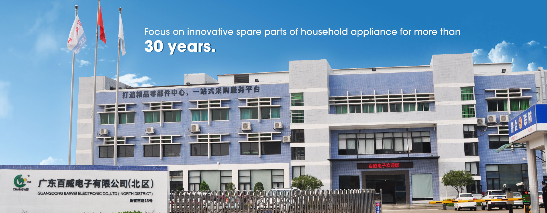
For over 40 years, electronics manufacturers have trusted and relied on Camptech II Circuits’ expertise and production capabilities to manufacture their printed circuit boards. Whether your PCB is a simple one layer design or you require a multilayer boar

This company is MIL-PRF-31032, MIL-PRF-55110G, AS9100C, ISO 9001:2008 Certified, IPC 6012 Class 2, 3 and 3A Qualified, and ITAR Registered. They operate divisions in Aurora, CO, Tempe, AZ, and Maple Grove, MN. Advanced Circuits offers printed circuit boar

How PCB is Made in China - NextPCB Factory Visit || PCB Manufacturing & Assembly Process

PCB manufacturing involves converting design files which include Gerbers and netlists into a physical circuit board on which components can be placed and soldered. The fabrication process begins with design output files (Gerbers, netlist, drill files, et

A. Design and board output files Manufacturing commences soon after receiving the design files from a PCB designer. The designer creates the output files in Gerber or ODB++ format for fabrication and the bill of materials (BOM) for assembly.

The manufacturer performs DFM checks to identify potential risks and errors that might arise during the fabrication process. In case of any errors, the designer/customer is alerted about it. The corrected files are then fed to the CAM (computer-aided manu

B. Inner layer imaging Due to miniaturization, fabricators mostly use LDIs (laser direct imaging). They also use a special printer called plotter, which makes photo films of the circuit layers, solder mask, and silkscreen layers to print the circuit image

After developing the image, the unhardened photoresist (that protects the desired copper) is removed with an alkaline solution. C. Etching In PCB fabrication, etching is a process of removal of unwanted copper (Cu) from the board. The unwanted copper is

The important parameters to be considered during the etching process are the rate of panel movement, spray of chemicals, and amount of copper to be etched off. The whole process is implemented in a conveyorized, high-pressure spray chamber. D. Photoresis

H. Drilling During the drilling process, holes for vias and leaded components are drilled. An X-ray drill locates targets in the inner layer. The machine drills registration holes precisely. This machine is computer-controlled in which an operator can se

. Electroless copper deposition The first step in the plating process is to make the hole barrel conductive by means of chemical deposition of a very thin layer of copper on the hole walls. This process is called electroless copper deposition. This reacti

Outer layer imaging We used photoresist on the panel for inner-layer imaging. Similarly, imaging will be conducted for the outer layers of the panel using a positive image. Here, the process follows print-plate-etch method. The first step involves cleanin

Photoresist stripping Once the panel has been plated the photo-resist becomes undesirable and needs to be stripped from the panel in order to expose the unwanted copper. Here, a single continuous process line is used to dissolve and wash off the resist wh

Profiling and v-scoring Circuit boards are profiled and cut out of the production panel in the final manufacturing stage. The method employed either uses a router or a v-groove. The v-groove cuts diagonal channels on both sides of the board, while the rou

 pcb manufacturing companies